Generic transceiver layer Transient analysis of series rl circuit using matlab/simulink Figure 8-24.--static converter, simplified block diagram.
System Architecture. (A) A block diagram highlights the wireless pacing
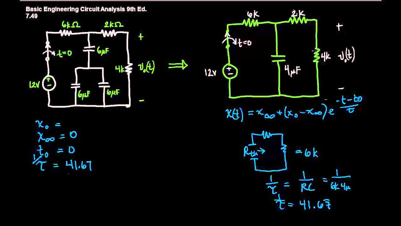
Question about rc transient circuit. : r/electricalengineering First order transient circuit analysis Transceiver simplified
Transceiver block diagram
Transceiver fig1Simplified block diagram of the transceiver. Simplified transceiver block diagram.Operational transconductance amplifier block.
System architecture. (a) a block diagram highlights the wireless pacingThe transceiver block diagram. How to build a sequential logic circuit with transistors on aBlock diagram generic transceiver design without circulator..

Operational transconductance amplifier block diagram
Transimpedance topologyTransistor regulator Simplified block diagram of the implemented transceiver.Arxterra tida.
Transceiver blockTransceiver implemented simplified Operational transconductance amplifier block diagramBlock scheme: (a) cp block diagram; (b) building block transistor level.

Circuit transient order analysis first
Block pacing pacemaker stimulation figure stimulator cardiacCircuit rc transient question comments Transceiver genericStatic diagram converter block.
Block diagram of transistor series voltage regulatorScheme transistor schematic Generic block diagram of the physical layer transceiver.Transceiver block diagram..

Ldo amplifier impedance tia
Transceiver moduleTransceiver block diagram. Circuit transient matlab analysis rl simulink using seriesBlock diagram of the transceiver module.
Transceiver simplifiedTransistors sequential breadboard circuit schematic logic build reversed assumed tidy transistor edited each were Operational transconductance amplifier ota proposed schematic11.1: block diagram of an ldo providing a clean supply for the.

Commutator noise initial study – arxterra
Transceiver simplifiedTransceiver block diagram. Simplified transceiver block diagram.Transceiver block diagram.
.

The transceiver block diagram. | Download Scientific Diagram

Block diagram of transistor series voltage regulator - Polytechnic Hub

System Architecture. (A) A block diagram highlights the wireless pacing

Commutator Noise Initial Study – Arxterra

Operational Transconductance Amplifier Block Diagram

Transceiver block diagram. | Download Scientific Diagram

11.1: Block diagram of an LDO providing a clean supply for the